| Author |
 Topic Topic  |
|
|
notburnin

Canada
3 Posts |
 Posted - 03/30/2009 : 13:20:59 Posted - 03/30/2009 : 13:20:59


|
Hi;
I have been unable to successfully flash with a new programmer.
H/W Re: GQ-4X Re-1.10
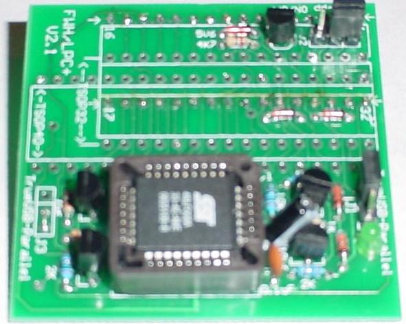
FWH/LPC+V2.1 adapter
<<SST49LF008A*PLCC32>> SST49LF0008A 33-4C-NHE 0835108-B PLCC32
Upgraded the software to:
USB Driver Re.2.01
Software Re. 4.01
I have approximately 40 write failures with 4 new chips. (no successes)
Failed writes occurred at different addresses.
9VDC, 200ma, positive, 2.1mm power adapter
Tried all write speeds
Tried reseating ZIF adapter and PLCC barely in socket as suggested.
Performed ID Check, Erase, Blank Check (successfully) before failed writes.
Scanned the FAQs/forums.
I have used various other programmers over the years.
I have NOT seen the VPP LED flash.
I have NOT touched the adapter jumpers yet.
Any help would be appreciated.
Thanks |
|
| Reply #1
ZLM
    
2949 Posts |
 Posted - 03/30/2009 : 16:02:01 Posted - 03/30/2009 : 16:02:01


|
1, No power adapter needed.
2. Set the J1,J3 jumpers to True-USB position.(1-2)
3. Set Jumper J2 to VPP ON position.
4. Should get ID correctly.
5. Do not push the chip too deep in the socket, barely put the chip in the socket will help the contacting.
The VPP LED should on on this chip.
Did you ever programmed any other chips? What they are?
|
 |
|
| Reply #2
notburnin

Canada
3 Posts |
 Posted - 03/30/2009 : 19:57:49 Posted - 03/30/2009 : 19:57:49


|
quote:
Originally posted by ZLM
1, No power adapter needed.
2. Set the J1,J3 jumpers to True-USB position.(1-2)
3. Set Jumper J2 to VPP ON position.
4. Should get ID correctly.
5. Do not push the chip too deep in the socket, barely put the chip in the socket will help the contacting.
The VPP LED should on on this chip.
Did you ever programmed any other chips? What they are?
Hi;
Thanks for the quick response.
I have attached a bad pic, sorry.
J1 appears to be jumpered 1-2
J3 arrived already pre-soldered 2-3
J2 appears to be jumpered 1-2 (Vpp on)
ID Check has always worked.
PLCC is barely in the socket. top of PLCC is approximatley 0-1mm above the top of socket.
I have programmed DIPs, TSOPs and a few PLCCs with other programmers such as old DataIO's and Xeltek's.
I have not burned any chip successfully with this programmer yet.
I could re-solder J3 to 1-2.
Darn, I thought the lack of Vpp LED was a bad sign.
Should I open the case to see if anything obvious is wrong?
Image Insert:

47.43�KB |
Edited by - notburnin on 03/30/2009 20:01:17 |
 |
|
| Reply #3
ZLM
    
2949 Posts |
 Posted - 03/30/2009 : 20:06:44 Posted - 03/30/2009 : 20:06:44


|
The Vpp should not ON, it is not used on this chip. The programmer is good. The problem is the adapter J3. If you select menu item Test H/W voltage, then you will see the Vpp is working.
Please resolder the J3 to True-USB pin 1-2. |
 |
|
| Reply #4
notburnin

Canada
3 Posts |
 Posted - 03/30/2009 : 23:37:23 Posted - 03/30/2009 : 23:37:23


|
quote:
Originally posted by ZLM
The Vpp should not ON, it is not used on this chip. The programmer is good. The problem is the adapter J3. If you select menu item Test H/W voltage, then you will see the Vpp is working.
Please resolder the J3 to True-USB pin 1-2.
Resoldered J3 to pin1-2,
First chip completed using speed +2(no errors) and booted.
I previously did check the Test H/W voltage.
By the way, info for the adapter lists:
Vpp: 12V
ReadVpp: not set or invalid
It was unclear if it was used and I had not checked the datasheets.
Also: How does the programming speed (-2, -1, 0, +1, +2) correspond to a particular chip write speed?
Thanks
Great service! |
 |
|
| Reply #5
ZLM
    
2949 Posts |
 Posted - 03/30/2009 : 23:51:23 Posted - 03/30/2009 : 23:51:23


|
ReadVpp parameter is not used on this chip.
The speed adjustment is only providing a chance for increasing the compatibility of the chip.
So, keep +2 if the chip write successfully. If fails write, then try to reduce the speed.
|
 |
|
| |
 Topic Topic  |
|
|
|

